|
Versione inglese ed italiana
Vers. 2.00
Cosč un line
driver?
Richiesta informazioni. Applicazioni
|
|
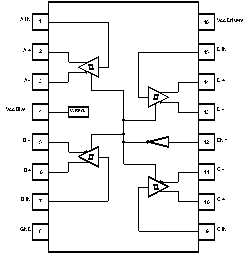
CIRCUITO
INTEGRATO LINE DRIVER DIFFERENZIALE - Quattro amplificatori con logiche e
soglie separate e funzione di abilitazione. Vers. LF compatibile con le
normative RoHS
QUAD
DIFFERENTIAL LINE DRIVER
WITH
SEPARATE LOGIC BIAS AND DRIVER BIAS CONNECTIONS, AND ENABLE FUNCTION. RoHS
compliant Lead Free
FEATURES
-
Supply
 (Bias) Voltage Range 3.5V to 30V (Bias) Voltage Range 3.5V to 30V
-
Operation to 800 KHz
-
Separate logic bias and driver supply pins
-
Optional single supply operation for moderate power
applications
-
High impedance Buffered Inputs with Hysteresis may be
driven directly by phototransistors
-
Tri-State ouputs
-
80 mA peak
SINK/SOURCE current
-
Outputs Protected by Thermal Shut-Down
ŘĽ/span>: Negazione / not
|
DESCRIPTION
These Line drivers are pin
compatible with 26LS31 in applications wher pin 4 = 5V and pin 12 =
GND. Internal clamp diodes allow trouble-free operation when driving
cable lengths exceeding 100mt. Split supplies are provided to
minimize standy power dissipation in high voltage applications. The
logic should be powered from a regulated 5V supply at the VccBias
pin. The output stages may then powered by a separate supply at
VccDrivers, up to 30V. Output voltage swings of 0.3V to Vcc-1.9V are
typical. The outputs are protected against shorts to ground, shorts
to Vcc and to other outputs, by a two-fold scheme of current
limiting and thermal shutdown. This assures highly reliable
operation in harsh environments. Heat-sinking may be accomplished at
pin 8 wich is directly connected to the ASIC substrate.
DESCRIZIONE
Il circuito integrato presentato in questa pagina, comunemente
chiamato line driver, ?n buffer o un amplificatore evoluto,
ideale per applicazioni industriali. Molto potente, veloce e robusto
consente di pilotare rapidi segnali in ambienti ostili ricchi di
rumore elettromagnetico.
Il line drivers MO-ET7272B (MO-ET7273B versione open collector) 荊 compatibile con il 26LS31 in applicazioni ove il pin 4 ?ari a +5V
ed il pin 12 ?osto a massa. Diodi interni, consentono di evitare
problemi quando si pilotano, ad alta frequenza, carichi fortemente
induttivi e/o capacitivi come cavi lunghi oltre i 100 metri. Le
alimentazioni sono separate per ridurre il consumo in applicazioni
ad alta tensione. Infatti la logica ?ilotata con una tensione di
alimentazione pari a 5V dal piedino VccBias, mentre gli stadi di
uscita possono essere alimentati con una tensione di alimentazione
pari ad un massimo di VccDriver = 30V. Tipicamente, gli stati
d'uscita vanno da 0,3V a (+Vcc-1.9V). Le uscite sono protette contro
i corto-circuito a massa, verso +Vcc e verso le altre uscite,
tramite un circuito di limitazione della corrente ed un sistema di
spegnimento sensibile al calore. Tutto questo consente di garantire
ottima affidabilit?nche negli ambienti pi?ifficili ed
aggressivi senza deteriorare le ottime performance. L'ASIC ?on
package in cui viene garantita un'ottima dissipazione del calore
direttamente dal bulk del silico.
|
ABSOLUTE
MAXIMUM RATINGS
|
Parameters
|
Symbol
|
Min.
|
Typ.
|
Max.
|
Units
|
Ref
|
|
|
TA
|
-55
|
|
115
|
?C
|
Note 1
|
|
Supply (Driver) Voltage Range
|
TCCD
|
4.5
|
|
30
|
V
|
|
ELECTRICAL CHARACTERISTICS
Unless otherwise specified,
TA = 25?C and EN -<0.8V.
|
Parameters
|
Symbol
|
Min.
|
Typ.
|
Max.
|
Units
|
Test Conditions
|
|
|
TJOP
|
|
172
|
|
?C
|
Note 1
|
|
Over Release Point
(junction)
|
TJRP
|
|
136
|
|
?C
|
Note 1
|
|
Vcc Bias Voltage Range
|
VCCB
|
3.5
|
5
|
30
|
V
|
|
|
Vcc Drivers Voltage Range
|
VCCD
|
4.5
|
5
|
30
|
V
|
|
|
Supply Current VCCB1
(Bias)
|
ICCB1
|
|
11.9
|
16.0
|
mA
|
VCCB and VCCD = 5V
|
|
Supply Current VCCD1
(Drivers)
|
ICCD1
|
|
2.4
|
3.3
|
mA
|
VCCB and VCCD = 5V
|
|
Supply Current VCCB2
|
ICCB2
|
|
2.5
|
3.4
|
mA
|
VCCB and VCCD = 5V, EN- > 2V
|
|
Supply Current VCCD2
|
ICCD2
|
|
0.0
|
0.1
|
mA
|
VCCB and VCCD = 5V, EN-> 2V
|
|
Supply Current VCCB3
|
ICCB3
|
|
12.1
|
18.5
|
mA
|
VCCB and VCCD = 30V
|
|
Supply Current VCCD3
|
ICCD3
|
|
2.4
|
3.3
|
mA
|
VCCB and VCCD = 30V
|
|
Supply Current VCCB4
|
ICCB4
|
|
3.6
|
3.5
|
mA
|
VCCB and VCCD = 5V, EN- > 2V
|
|
Supply Current VCCD4
|
ICCD4
|
|
0.0
|
0.1
|
mA
|
VCCB and VCCD = 5V, EN- > 2V
|
|
Enable Input Tresholsd
|
VTHE
|
0.8
|
1.5
|
2
|
V
|
|
|
Enable Low Level Input Current
|
IILE
|
-10
|
0
|
10
|
mA
|
VIN
= 0V, VCCB = 5V
|
|
Enable High Level Input Current
|
IHE
|
|
108
|
150
|
mA
|
VIN
= 5V, VCCB = 5V
|
|
High Impedance Output Leakage
|
IOZ
|
-4.0
|
0.0
|
4.0
|
mA
|
VCCD = 30V, EN-> 2V,
Output at 15V
|
|
Input Positive-Going Treshold
|
VT+
|
1.05
|
1.25
|
1.45
|
V
|
VCCB = 5V
|
|
Input Negative-Going Treshold
|
VT-
|
0.75
|
0.95
|
1.15
|
V
|
VCCB = 5V
|
|
Input Hysteresis
|
VH
|
|
0.3
|
|
V
|
VCCB = 5V
|
|
Low Level Input Current
|
IIL
|
|
-0.1
|
-4.0
|
mA
|
VIN
= 0V, VCCB = 5V
|
|
High Level Input Current
|
IH
|
|
0
|
4.0
|
mA
|
VIN = 5V, VCCB = 5V
|
|
Low Level Output1
|
VOL1
|
|
375
|
500
|
mV
|
IOL
= 20 mA, VCCD
= 5V
|
|
Low Level Output2
|
VOL2
|
|
370
|
500
|
mV
|
IOL
= 20 mA, VCCD
= 30V
|
|
High Level Output1
|
VOH1
|
2.4
|
2.8
|
|
V
|
IOH = 20 mA, VCCD = 5V
|
|
High Level Output2
|
VOH2
|
27.7
|
28.1
|
|
V
|
IOH = 20 mA, VCCD = 30
|
|
Parameters
|
Symbol
|
Min.
|
Typ.
|
Max.
|
Units
|
Test Conditions
|
|
|
TPLH
|
|
450
|
630
|
ns
|
|
|
Propagation delay, falling input 50% point to zero
crossing of differential outputs
|
TPHL
|
|
450
|
630
|
ns
|
|
|
Output Rise Time
|
TR
|
|
700
|
980
|
ns
|
|
|
Output Fall Time
|
TF
|
|
700
|
980
|
ns
|
|
|
|