|
|
|
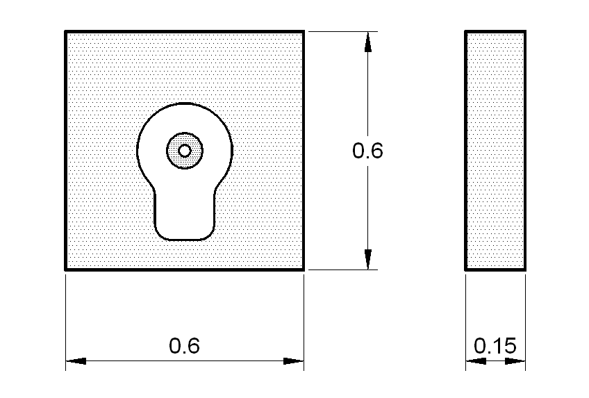
Emettitore ad alte prestazioni: VCSEL –
Chip (DVE03)
- Emettitore NIR VCSEL 850 nm
- Bassa corrente
- Alta velocit༯font>
- High performance Emitter: VCSEL Dice (DVE03).
- VCSEL Infrared 850 nm Emitter
- Low Current
- High Speed
ELECTRO-OPTICAL CHARACTERISTICS (T=25?C unless otherwise specified)
PARAMETER |
SYMBOL |
UNITS |
MIN. |
TYP. |
MAX |
NOTE |
| Peak Wavelength |
Lambda p |
nm |
 |
850 |
|
|
| Threshold Current |
Ith |
mA |
|
|
2 |
|
| Output Power at High Current |
P1 |
mW |
1,8 |
5 |
|
High Current Defined As I1=20mA |
| Slope Efficiency |
D P1/D
I |
mW/mA |
|
0,5 |
|
|
| Operating Voltage at Low Current |
V0 |
V |
|
|
2,0 |
Low Current Defined As I0=9mA |
| Differential Resistance |
d R |
ohm |
|
40 |
65 |
|
| Reverse Bias Voltage |
Vrev |
V |
5 |
|
|
|
| Total Beam Divergence |
tetha |
deg |
|
20 |
|
|
ABSOLUTE MAXIMUM RATINGS (T=25?C unless otherwise stated)
PARAMETER |
RATING |
| Storage Temperature |
-40 to
+100?C |
| Operating Temperature |
0 to
70?C |
| Maximum Die Exposure |
325?C
for 10 sec |
| Maximum Optical Output Power |
10 mW |
| Maximum Revers Bias Voltage |
5 V |
| Maximum continuous Operating
Current |
20 mA |
| Maximum Instantaneous Operating
Current |
25 mA |
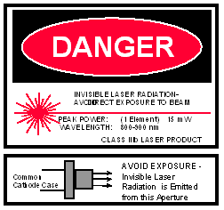
MOLTO IMPORTANTE
Con "Absolute Maximum Ratings" si intendono i limiti del
dispositivo oltre i quali si rischia di danneggiare o addirittura distruggere il
dispositivo.
ATTENZIONE:
LASER semiconduttore classe 3B Evitare assolutamente l’esposizione diretta alla
radiazione invisibile (NIR).
IMPORTANT NOTICE
| Stresses beyond those listed under
"Absolute Maximum Ratings" may cause permanent damage to the device. These are
stress only, and functional operation of the device at these or any other conditions
beyond those indicated for extended periods of time may effect device reliability. WARNING: Semiconductor LASER Class 3B device. Avoid exposure, invisible LASER radiation
is emitted
Micropto S.r.l. reserves the right to make changes in order to
improve design and supply the best product possible. |
|
|